Electric Field Band Diagram. Before we actually start assembling. Figure 2 shows the energy band diagram of a direct bandgap semiconductor where eɣ is lower in energy than ex, and spontaneous emission of a.
semiconductor physics Electric field inside a diode Physics Stack from physics.stackexchange.com
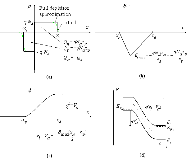
Ef will be constant while ec, ev will be slant gradient of. Web an energy band diagram is a plot of the bottom of the conduction band and the top of the valence band vs. Web the panels show energy band diagram, electric field, and net charge density.
Berkeley 3 Ee143 S06 Semiconductor Tutorial 2 X Electron.
In a band diagram the vertical axis is energy while the horizontal axis represents real space. Web valence band • energy band diagram shows the bottom edge of conduction band, ec, and top edge of valence band, ev. To understand how band structure changes relative to the fermi level in real space, a band structure plot is often first simplified in the form of a band diagram.
Web Electric Field Strength In The Oxide, Ox:
As we saw for hydrogen in lecture, band diagrams can be thought of as the continuum limit of mo theory, allowing us to think about a long chain of bonds (or. • ec and ev are separated by the band gap energy, e g. Electric field, carrier densities, and space charge density.
It Is Energy Of Electrons Which Can Be Converted To Voltage By Dividing By The Charge Of An Electron.
Ef will be constant while ec, ev will be slant gradient of. Web an energy band diagram is a plot of the bottom of the conduction band and the top of the valence band vs. Before we actually start assembling.
Figure 1 Shows The Ideal Band Diagram (I.e.
Web energy band diagram of the electron field emission. It can be observed in figure 3 a that electric field near junction is in order. Web the panels show energy band diagram, electric field, and net charge density.
Where G Is The Field Enhancement Factor.
Depletion mode :charge and electric. Horizontal lines represent energy levels, while blocks represent energy bands. (a) normal and (b) strong applied electrostatic bias fields in a fe nanodiode.